1. Target device : Cyclone V SoC
2. External Memory : DDR3 1Gb
The design leverages the ability for users to send Avalon® Memory Mapped commands over JTAG. The Avalon-MM commands are routed to a JTAG to Avalon Master Bridge, which is tied to the FPGA To HPS AXI™ Bridge on the HPS. From there the data is directed into the L3 Interconnect where it is routed based on the destination address. A command with the appropriate destination address is routed to the SDRAM Controller Subsystem where it will ultimately be executed.
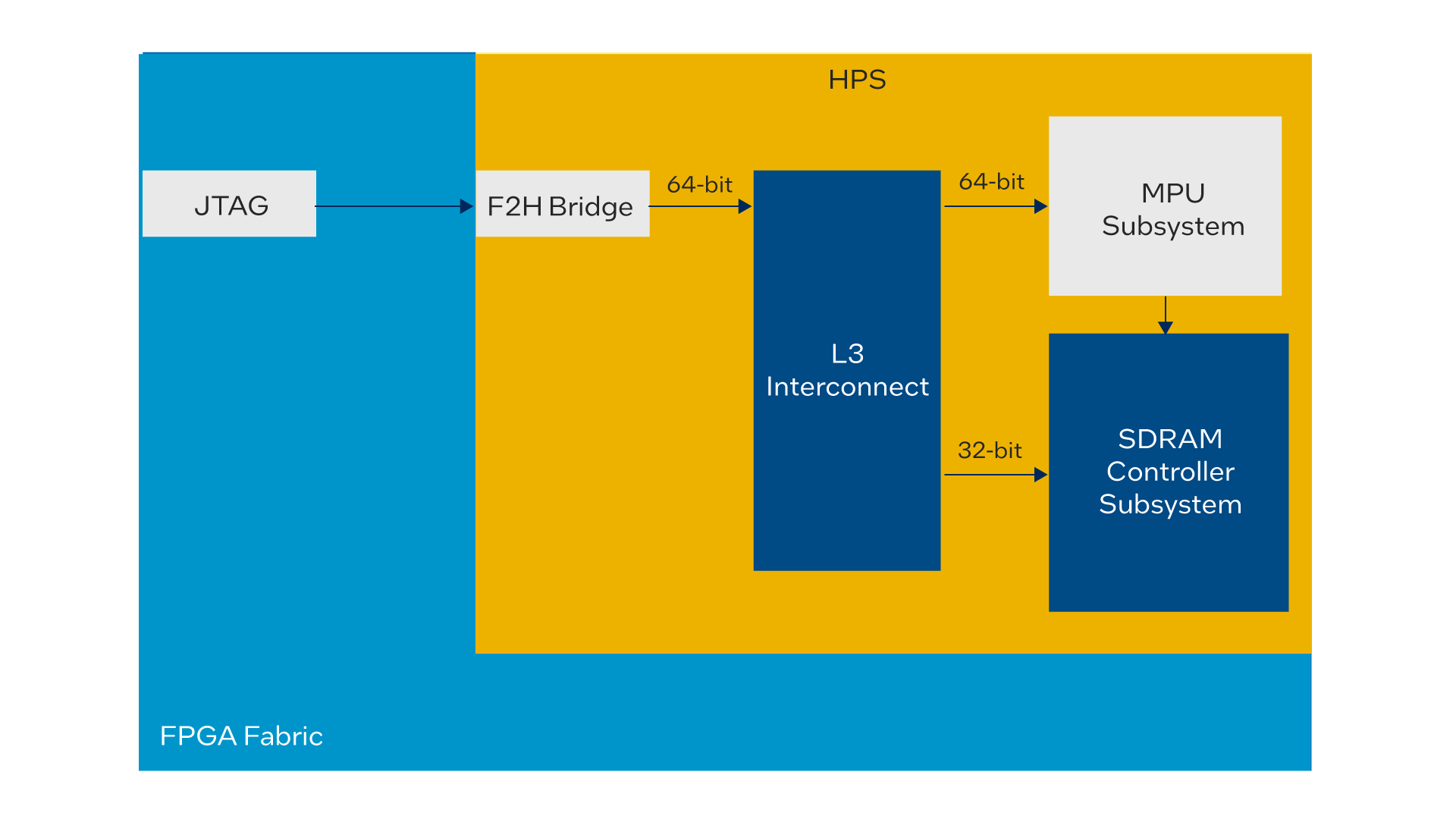
Figure 1. Design Example Block diagram
The 1GB of memory is partitioned using two rules. The first rule sets the access region for the MPU. The MPU is granted access from 0MB to 512MB. The second rule sets the access region for the L3 Interconnect. The L3 Interconnect has access from 319MB to 1,024MB. The overlap of these two rules results in a "Shared" region which both the MPU and L3 interconnect can access.

Figure 2. Design Example Memory Partitions
Using This Design Example
Download the Cyclone V Memory Partition design example (.zip file)
Download the Cyclone V Memory Partition design example readme (.txt file)
https://www.altera.com/support/support-resources/design-examples/soc/shared-memory-partition.html
'[FPGA]' 카테고리의 다른 글
| Altera DE0 FPGA 보드의 핀맵 (0) | 2019.02.28 |
|---|---|
| [altera] Warning: Time value "xxx" truncated to "xxx" (0) | 2018.12.11 |
| verilog 합성 기초 로직 설명문서 (0) | 2018.02.28 |
| [xilinx] fatal_error:maphelpers:basmpreport.c:214:1.18 :: 대응방법 (0) | 2017.08.30 |
| Altera(Intel FPGA) Configuration 과정 (0) | 2017.07.04 |