Imagine traveling back in the time to the early human ages. It’s going to be both scary and interesting when you meet a person who probably cannot speak or if they do you won’t be able to understand them. Clearly, communication will not be possible until you find a mutual way to convey your respective meanings/intentions. The same principle applies in the world of electronics as there are various types of interfaces among electronic devices. Therefore, a standard communication protocol eases the transformation of data in a system, especially in a System-on-Chip (SoC) system which consists of different systems.
SoC FPGAs such as Xilinx® Zynq™ establishes the ARM Advanced Microcontroller Bus Architecture (AMBA) as the on-chip interconnection standard to connect and manage the functional blocks within the SoC design. The Advanced eXtensible Interface (AXI) is designed for FPGAs based on AMBA as a protocol for communication between blocks of IP.
Here are some of the important features of an AXI interface:
- It supports burst transactions with only start address issued
- There are different phases for the data and addresses
- Write and read channels are separated which causes the low-cost Direct Memory Access (DMA)
- Transactions can be completed out of order
- Multiple outstanding addresses can be issued
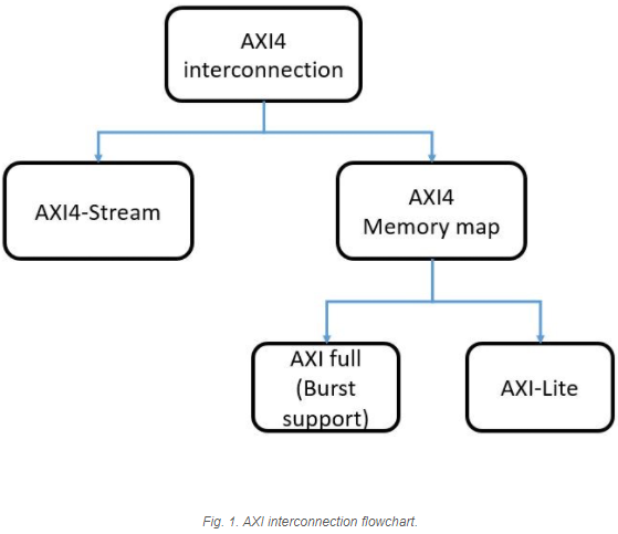
Regarding the nature of the design, there are two types of AXI4 interface which are shown in Fig. 1. Namely, AXI4 memory map (AXI4 or AXI4-lite) and AXI4-stream.
- AXI4: Capable of doing memory map burst transaction up to 256 data transfer cycles per address phase.
- AXI4-Lite: Utilized for the single bit memory map transaction.
- AXI-Stream: There is no address channel and it allows an unlimited burst transaction between the master and slave.
AXI transaction channels
The AXI write and read transaction channels are summarized into 5 categories. In the following text I won’t explain all of the signals in each transaction, just the ones I consider most important (for the purpose of this blog). Fig. 2 shows an AXI interconnection IP and its associated ports in the Xilinx Vivado suite design.
- Writing address channel: At the beginning of the transaction, the master drives the slave by sending the AWVALID which says there is a write transaction ready. After that the address to be written will be sent by AWADDR to the slave. Then, the response from the slave will come through the AWREADY signal. There is also the AWLEN, in which we define the number of transfers in a burst. The AWSIZE is used to clarify the size of each transaction, e.g. 32 bits. Each transaction has its own ID that will be sent through the AWID to the slave.
- Writing data channel: By ending the address transaction, WVALID, WREADY and WDATA will be done the same as for the writing address channel. The last transaction in a burst is defined through the WLAST signal. WSTRB says which bit of a bus is used for the transactions which is useful when the bus is 32 bits and the data is just 2 bits.
- Write response channel: used to inform the master about the status of the write transactions. BVALID is sent by the slave and says that ‘I am ready to send the response’. The response from the master will be sent through the BREADY. The response is sent through the BRESP.
- Read address channel: As with the write address channel, the ARVALID, ARADDR, ARSIZE, ARLEN, ARID and other signals are the same.
- Read data channel: There are RDATA, RID, RLAST, RVALID and RREADY that are the same as the writing data channel. The status of the read transfer is identified in the RRESP.

Communication interfaces between Programmable Logic (PL) and Processing System (PS)
There are a number of special ports within the Zynq architecture that are intended for establishing communication between the PS and PL sides of the device. Fig. 3, shows the structure of these ports.
- AXI_GP: These ports are used for the general purpose application between the PL and PS. These are the main ports for the PS to access the PL and vise verse.
- High performance (HP): These memory map connection ports provide a high bandwidth data-path from the master modules in PL to the D-ram and on-chip memory (OCM) in PS.
- Accelerator Coherency Port (ACP): This port provides access to the memory subsystems from the PL to the PS. Through this port, the PL can access the cache memories inside the PS which improves overall performance and power consumption.

The AXI Interconnection is the established language between PS and PL of Zynq. The FPGA vendors such as Xilinx has amazingly made possible to combine software and hardware subsystems within a single chip, and AXI is the main system of communication between these subsystems. As a SoC designer, understanding the AXI Interconnection is a must.
참조 : www.aldec.com/en/company/blog/145--demystifying-axi-interconnection-for-zynq-soc-fpga
'[FPGA]' 카테고리의 다른 글
| Error (329006): Some pins have illegal board trace modelsDescription (0) | 2022.07.19 |
|---|---|
| MGT(Multi-Gigabit Transceiver) PCS, PMA (0) | 2021.10.29 |
| [Intel FPGA] AVMM master templates (0) | 2020.07.02 |
| Intel FPGA (altera) Introduction to FPGA HIGH SPEED IO (0) | 2020.07.02 |
| [FPGA] pre-emphasis 란.. (0) | 2020.05.29 |