abstract
The implementation of image edge detection on hardware is important for increasing processing speed of image processing systems. The project implements edge detection using Sobel Operator on a Field Programmable Gate Array device. Edge information for a particular pixel is obtained by exploring the brightness of pixels in the neighbourhood of that pixel. Measuring the relative brightness of pixels in a neighbourhood is mathematically analogous to calculating the derivative of brightness. The pixel information extracted is transferred from the computer to the field programmable gate array device. Sobel edge detection operations are performed on the data and the processed data is sent back to the computer. The transfer of data is done using parallel port interface operating in bidirectional mode. All the digital logic implemented and verified on the field programmable gate array kit was described using the Verilog® Hardware Description Language and the target was Xilinx Spartan 3 Family device XC3S400. The functional verification and simulation was performed using free and open source electronic design automation tools, GPLCver for Verilog compilation and GTKWave for post processing of simulation results. Conversion of image to raw format and creating the output image is done using software written in C. Xilinx Integrated Software Environment suites of tools were employed for synthesis, mapping, placement and
route and for configuring the target device.
Edge Detection Hardware Architecture
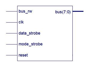
The Block gives the overall I/O ports on the edge detection system using fpga.
The bus_rw controls the direction of data transfer while data_strobe and mode_strobe signals control the entire data transfer operation. The clk signal is the internal clock of the FPGA. The bus(7:0) is an 8 bit bidirectional data bus.
Internally the system consists of Ram Modules wired to 32 FPGA modules. There are 3 sets of 34byte RAM array which can be serially loaded and parallely shifted. The 3 sets of RAM Array are wired to 32 Sobel Instances
P0, P1, P2, P3, P4, P6, P7 and P8 represents the eight 8bit pixel inputs to the Sobel Module.  The module consists of signed subtractors, shift registers and modulus operators. The output of the final adder block will be 11 bits (10 bits for the data as the maximum value of the adder output is 4*255 and the 11th bit as the sign bit). The output data is compared to limit the value to a maximum of 255 as the output image is also composed of 8-bit wide pixels. 32 Sobel modules are used in parallel. The limitation on the number of parallel Sobel operators that can be implemented is logic resources available in the target device.
The Sobel output for one group of pixels calculated as per |Gx| + |Gy|.

The summary of the Sobel module showing the input output buses are shown above.
FPGA Statistics
A single Sobel operator logic consumes 149 four input lookup tables (LUT) which is 2% of the available FPGA resources.
| SOBEL Project Status | |||
| Project File: | sobel.ise | Current State: | Synthesized |
| Module Name: | sobel |
|
No Errors |
| Target Device: | xc3s400-4tq144 |
|
4 Warnings (0 new, 0 filtered) |
| Product Version: | ISE, 8.1i |
|
Sat Feb 28 16:13:45 2009 |
| Device Utilization Summary (estimated values) | |||
| Logic Utilization | Used | Available | Utilization |
| Number of Slices | 83 | 3584 | 2% |
| Number of Slice Flip Flops | 30 | 7168 | 0% |
| Number of 4 input LUTs | 149 | 7168 | 2% |
| Number of bonded IOBs | 74 | 97 | 76% |
| Number of GCLKs | 1 | 8 | 12% |
| Detailed Reports | |||||
| Report Name | Status | Generated | Errors | Warnings | Infos |
| Synthesis Report | Current | Fri Feb 27 20:56:01 2009 | 0 | 4 Warnings (0 new, 0 filtered) | 0 |
| Translation Report | |||||
| Map Report | |||||
| Place and Route Report | |||||
| Static Timing Report | |||||
| Bitgen Report | |||||
Sources
RAM MODULES
Three RAM modules each of size 3X34 are employed for storing the data from computer. The contents of the RAM modules are reset before initiating computation. When the control signals 몉eady� and 몉ead_write� are both asserted LOW, firstly the RAM module in the third row is loaded with 34 bytes of pixel values transferred from the computer via the parallel port. At the end of first data transfer operation, the contents of the RAM modules will be as follows:
| 00 | 00 | 00 | 00 | 00 | …………… | 00 | 00 |
| 00 | 00 | 00 | 00 | 00 | …………… | 00 | 00 |
| A1 | A2 | A3 | A4 | A5 | …………… | A33 | A34 |
Then the 몀ode_strobe� is asserted low after placing a value of 0110_0110 in the data bus. Then the entire rows are shifted one upwards. Then the third row is filled with next set of data values. Then the RAM module will be as shown in figure 5.3
| 00 | 00 | 00 | 00 | 00 | …………… | 00 | 00 |
| A1 | A2 | A3 | A4 | A5 | …………… | A33 | A34 |
| B1 | B2 | B3 | B4 | B5 | …………… | B33 | B34 |
Similarly after the third data transfer, the RAM will be as shown in figure 5.4 We start the edge detection operation as the entire RAM is ready. Consecutive three elements of each row will be the input to each of the 32 Sobel Modules. once the entire RAM is filled with valid data, only single shift need to be done to get the next set of valid data.
| A1 | A2 | A3 | A4 | A5 | …………… | A33 | A34 |
| B1 | B2 | B3 | B4 | B5 | …………… | B33 | B34 |
| C1 | C2 | C3 | C4 | C5 | …………… | C33 | C34 |
'[알고리즘]' 카테고리의 다른 글
| 행렬 제곱 계산 방법 (0) | 2012.10.25 |
|---|---|
| Convolution 개념 정리-이미지처리 기술 (0) | 2012.10.24 |
| 다양한 Edge(에지) 추출 알고리즘 : 1차미분, sobel, Prewitt, Roberts, Compass, Laplacian... (0) | 2012.10.22 |
| Harris Corner Detector 란 무엇인가 (0) | 2012.10.19 |
| Harris Corner Detection 관련된 논문 5 (0) | 2012.10.19 |